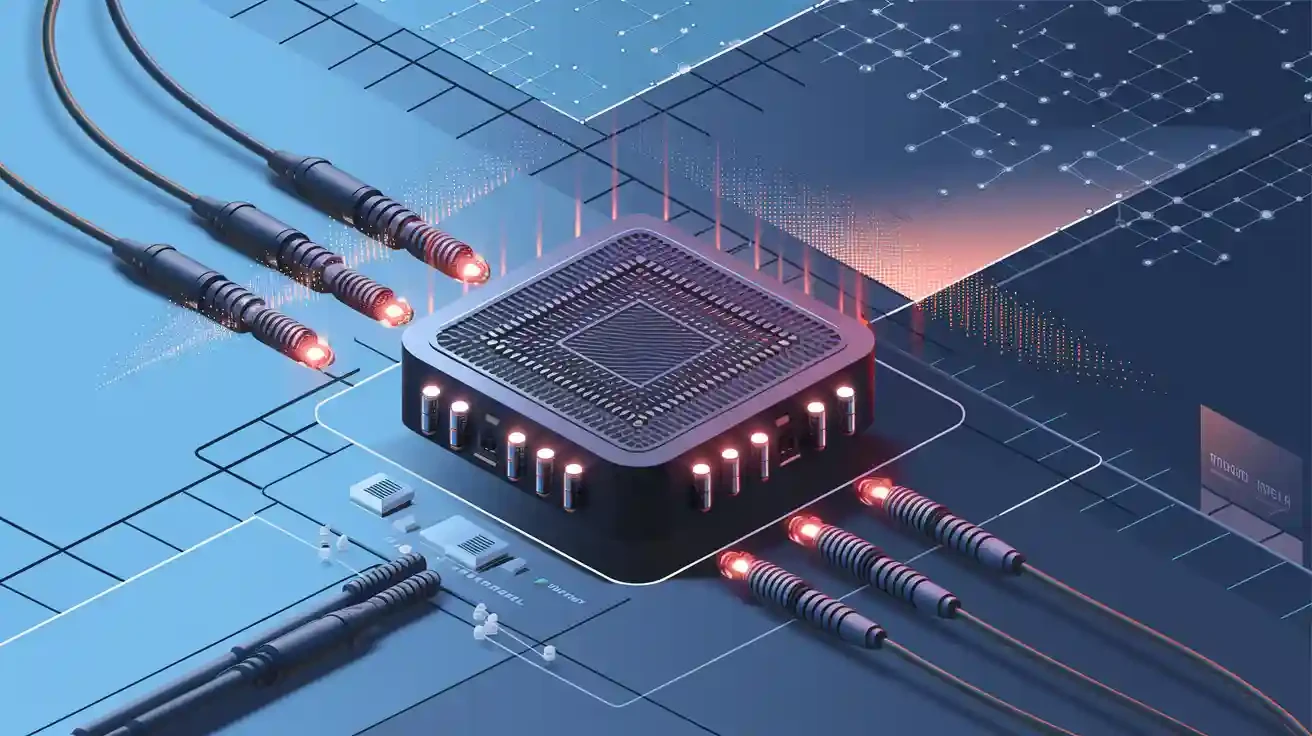
The leap from 100G/400G to 800G optical modules isn’t just about raw speed. It represents a fundamental shift in network infrastructure, largely driven by the explosive demands of AI workloads, hyperscale data centers, and the rollout of 5.5G/6G networks.
While much attention is paid to advanced DSPs (Digital Signal Processors), coherent optics, and silicon photonics, one critical component often works tirelessly in the shadows: the optical module housing.
This unassuming outer shell does far more than provide a physical cover. It is the first line of defense against overheating, a guardian of signal integrity, and a key to reliability. As data rates climb to 800G and push toward 1.6T, the housing is pushed to its physical limits, presenting engineers with a fascinating set of complex challenges.
1. The Thermal Wall: Managing Unprecedented Heat Density
The most immediate and severe challenge is managing heat.
Soaring Power Densities
800G optical modules, particularly those leveraging higher-power technologies such as Electro-Absorption Modulated Lasers (EML), generate significantly more heat than previous generations. Without efficient heat dissipation, the internal laser chips and processors risk overheating, leading to:
Degraded signal integrity
Reduced transmission performance
Dramatically shortened component lifespan
The Material Gap
Traditional housing materials (e.g., aluminum or zinc alloys) provided sufficient thermal performance for 100G–400G modules. However, at 800G and beyond, their thermal conductivity is often inadequate. This gap underscores the need for:
Advanced alloys with higher thermal conductivity
Materials optimized for lightweight design + efficient heat spreading
The Interface Bottleneck
Even if housing materials improve, heat transfer from chip to housing remains a bottleneck. This is where Thermal Interface Materials (TIMs) play a crucial role:
Standard TIMs may limit heat flow and create hotspots
Next-generation solutions—such as non-silicone, ultra-high-conductivity gels (≈12 W/m·K)—offer:
Better thermal transfer efficiency
Lower risk of optical contamination (avoiding silicone oil outgassing)
Improved reliability for high-power optical modules
2. Material Science: Pushing the Limits of Physics
To overcome the thermal wall, material science is being redefined.
The Rise of Advanced Alloys: Companies are innovating with new materials. For instance, Sirui New Materials has developed a tungsten-copper (CuW) alloy specifically for chip bases within these housings. This material addresses the need for low expansion and higher thermal conductivity, which is crucial for managing the heat of 400G+ modules. The manufacturing process requires extreme precision to avoid defects like porosity or tungsten particle agglomeration, which could impair performance.
Ceramics for High-End Applications: Ceramics are valued in high-end applications for their excellent thermal stability, good electrical insulation, and resistance to wear and corrosion.
The Composites Future: The future may lie in composite materials and hybrid designs, perhaps combining a metal base for optimal heat dissipation with other materials for weight or cost efficiency.
3. Precision Manufacturing: The Quest for Micron-Perfection
You can have the best material in the world, but if you can’t manufacture it precisely, it’s useless.
Tighter Tolerances: As internal components become more densely packed, the housing’s dimensional tolerances must become exceptionally tight. Any imperfection can misalign delicate optical components, reducing efficiency and increasing bit error rates.
Advanced Manufacturing Techniques: Producing these advanced materials requires sophisticated methods. Like 3D printing skeletons, vacuum melting infiltration directional solidification, and micro-precision machining to create their specialized CuW alloys, ensuring the necessary high cleanliness and density.
The Role of “Die Bonders”: The assembly process inside the housing is just as critical. Precision equipment like high-accuracy die bonders is essential. For example, Zhongke Precision’s new bonder achieves placement accuracy of ±1µm, which is crucial for aligning laser chips and other components within the tiny housing to ensure optimal performance and high production yields.
4. Signal Integrity at Breakneck Speeds: A Silent Guardian
At 800G using PAM4 modulation, data signals are incredibly fast and susceptible to interference.
EMI Shielding: The housing must act as a near-perfect Faraday cage, shielding sensitive internal signals from external electromagnetic interference (EMI) and preventing the module’s own emissions from disrupting nearby equipment. This requires continuous material and design optimization to maintain shielding effectiveness at higher frequencies.
Impedance Matching: The physical design of the housing, including its internal structures and connectors, must be engineered to maintain consistent impedance, preventing signal reflections that can degrade the integrity of high-speed electrical traces.
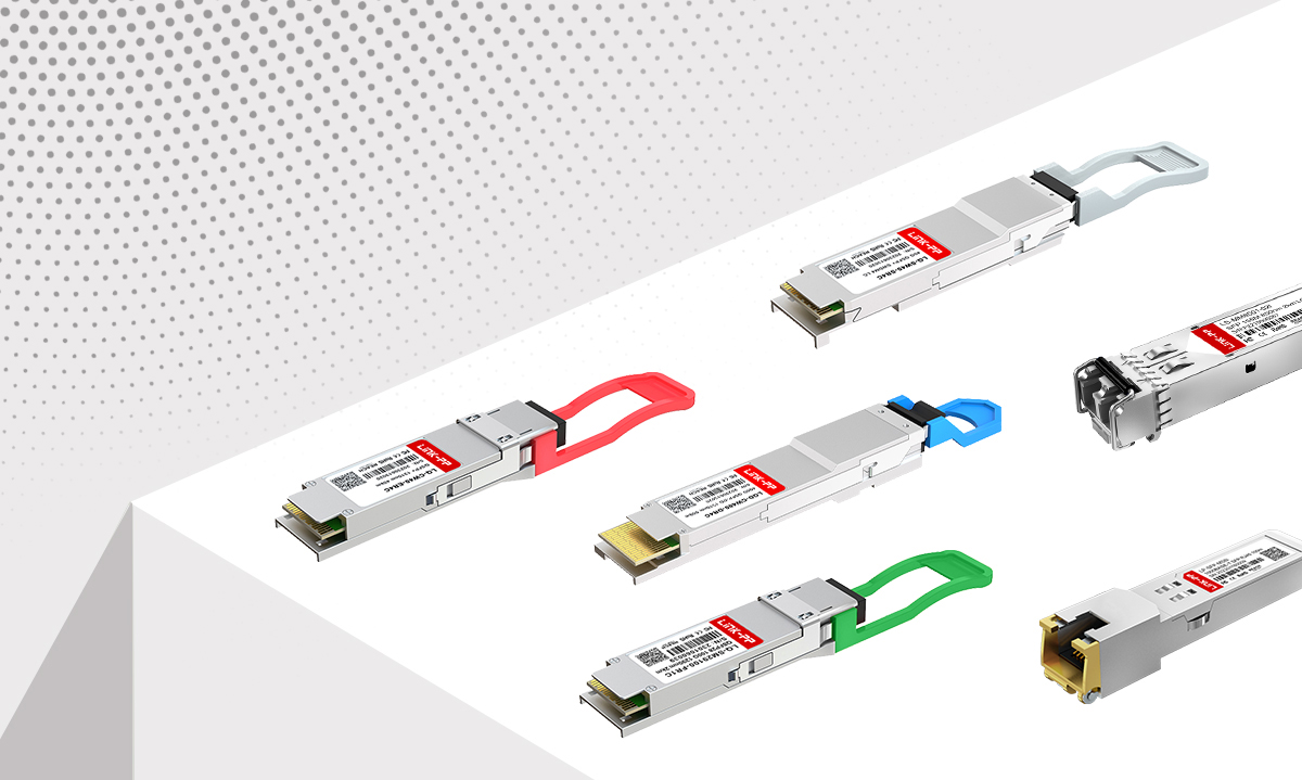
5. Standardization vs. Customization: The Form Factor Dilemma
The industry is navigating a split in packaging strategies, each with implications for housing design:
Feature | QSFP-DD800 | OSFP |
|---|---|---|
Size | Compact (18 × 89.5 mm) | Slightly larger (20 × 107 mm) |
Primary Advantage | Backward compatibility with 400G, higher port density | Superior thermal performance, future-proofing for 1.6T+ |
Power Handling | Lower | Higher (≥15 W), often includes an integrated heat sink |
Ideal Use Case | Data center spine-leaf networks, gradual 400G to 800G upgrades | New AI/HPC clusters, liquid-cooled data centers |
This duality means housing manufacturers must master two different design and thermal management philosophies.
Innovation in Action: How the Industry is Responding
Thankfully, the industry is not just facing these challenges but actively solving them through innovation:
Novel Thermal Materials: As mentioned, the development of new metal matrix composites (like CuW) and advanced TIMs is crucial for bridging the thermal performance gap.
Integrated Thermal Solutions: Housings are being designed with thermal management in mind from the start. The OSFP form factor, with its integrated metal heat spreader, is a prime example of this.
Liquid Cooling Compatibility: For the highest-power applications in AI clusters, housings are being designed to be compatible with direct-to-chip liquid cooling and immersion cooling systems, moving beyond traditional air cooling.
LINK-PP: Your Partner in Navigating the High-Speed Transition
At LINK-PP, we understand that selecting the right optical module is more than just choosing a speed. It’s about reliability, longevity, and total performance.
We closely follow these technological advancements and partner with suppliers who prioritize robust thermal design and housing integrity. Whether you are upgrading your existing data center with High-Speed modules or building a new AI-ready infrastructure with OSFP solutions, you can trust LINK-PP to provide modules engineered to overcome the challenges of the 400G/800G era.