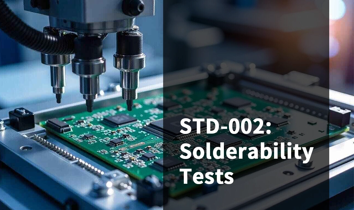
1. What is J-STD-002 and why it matters
J-STD-002 (EIA/IPC/JEDEC) defines standardized solderability tests for component leads, terminations, lugs, terminals and wires. It is the industry reference for qualifying whether a component’s terminations will reliably wet and form a good solder joint under realistic assembly conditions (dip, wave, or surface-mount reflow). It is an essential benchmark for ensuring strong, reliable solder joints in PCB assembly, minimizing the risk of defects, rework, and long-term failure.
Why solderability matters
Mechanical & electrical reliability — poor wetting → cold joints, increased contact resistance, intermittent failures.
Manufacturability — assemblies with poorly wetting components increase rework and scrap rates.
Supply-chain trust & compliance — customers, EMS houses, and regulators often require documented solderability evidence.
These motivations make a standardized approach like J-STD-002 essential in modern electronics supply chains
For manufacturers of networking and connectivity products—such as LINK-PP’s Integrated RJ45 connectors, LAN Transformers, Modular Jacks, and Fiber Optic Cages—adhering to J-STD-002 is a fundamental part of guaranteeing performance and durability in real-world applications.

2. Common test methods defined by the standard
J-STD-002 outlines multiple evaluation approaches:
Dip & Look (Solder Bath / Dip) — specimen is fluxed, dipped into molten solder at defined temperature and dwell time, then inspected under magnification. Good for through-lead and some leadless terminations.
Surface Mount Process Simulation (Test S / S1) — assembly simulation using printed solder paste and a reflow profile to evaluate SMT termination wetting (important for modern SMT connectors).
Wave / Solder Wave — simulates through-hole wave soldering for components intended for wave processes.
Wetting Balance (quantitative, if used) — measures wetting force/time and gives numerical curves (used in labs when quantification beyond visual pass/fail is needed).
3. Why solderability compliance matters
Consistent solderability ensures:
Secure mechanical connection between the component and PCB.
Low electrical resistance, preventing signal loss or heating.
Long-term reliability, even in high-demand environments.
For high-speed networking components like LINK-PP’s Integrated RJ45 modules or LAN Transformers, this reliability translates directly into stable data transmission and reduced maintenance costs. Similarly, Modular Jacks and Fiber Optic Cages that meet J-STD-002 standards integrate seamlessly into automated assembly processes with minimal risk of solder joint failure.
4. Example — LPJK0071AONL Integrated RJ45 Magnetics Jack
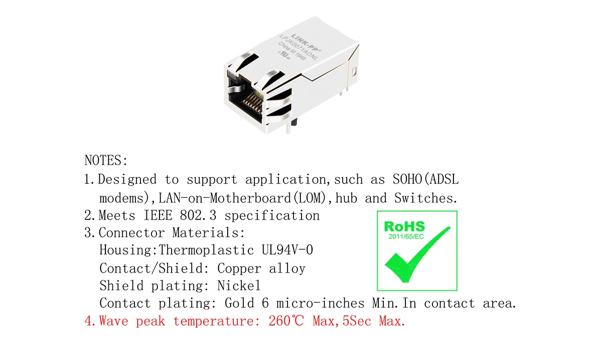
The LPJK0071AONL 1000 Base-T Integrated RJ45 Magnetics Jack is a prime example of LINK-PP’s commitment to solderability compliance:
Wave peak temperature: 260 °C max, 5 seconds max.
Designed for compatibility with wave soldering production lines.
Solderability verified to J-STD-002 standards upon request.
Compliance statement:
LINK-PP’s Integrated RJ45 connectors, LAN Transformers, Modular Jacks, and Fiber Optic Cages are designed and manufactured to meet J-STD-002 solderability requirements, ensuring dependable PCB integration.
5. Conclusion — Reliable solder joints, reliable networks
J-STD-002 provides a trusted, measurable benchmark for solderability. By designing Integrated RJ45 connectors, LAN Transformers, Modular Jacks, and Fiber Optic Cages to meet this standard, LINK-PP demonstrates engineering precision, quality control, and a commitment to customer satisfaction.