1. Introduction
As electronic devices become smaller, faster, and more powerful, traditional printed circuit boards (PCBs) often struggle to meet modern design requirements. This is where HDI PCB (High-Density Interconnect PCB) comes in. Known for its compact design, high wiring density, and superior electrical performance, HDI PCB has become a critical technology in smartphones, 5G networking, automotive systems, and beyond.
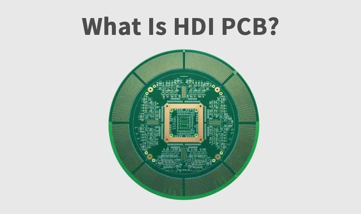
2. What Is an HDI PCB?
HDI PCB refers to a printed circuit board that uses advanced fabrication techniques such as microvias, blind and buried vias, fine lines, and sequential lamination to achieve higher interconnect density. Compared with conventional PCBs, HDI boards allow more input/output (I/O) connections in the same or smaller board area, making them ideal for today’s high-performance and space-constrained devices.
3. Key Features of HDI PCB
Microvias: Tiny vias typically under 0.1mm in diameter.
Blind & Buried Vias: Enable layer-to-layer connections without consuming surface space.
Fine Line/Spacing: Line widths and spacing down to 50–75μm or smaller.
Sequential Lamination: Multiple build-up layers for complex interconnections.
Any-Layer Interconnect (ALIVH): Direct routing between any PCB layers.
4. Advantages of HDI Technology
Miniaturization: Enables compact and lightweight device designs.
High-Speed Performance: Optimized impedance control reduces signal loss and crosstalk.
Greater Reliability: Microvias offer stronger mechanical stability under thermal stress.
Design Flexibility: Supports high-pin-count ICs such as BGA and CSP packages.
Better Electrical Properties: Reduced parasitic capacitance and inductance.
5. Manufacturing Process of HDI PCB
Laser Drilling for precise microvias.
Copper filling to ensure reliable interconnections.
Sequential Lamination to build multilayer structures.
Fine-Line Etching for dense circuit routing.
6. Applications of HDI PCB
HDI PCBs are widely adopted across multiple industries:
Consumer Electronics: Smartphones, tablets, wearables, and laptops.
Telecommunications: 5G base stations, routers, and network switches.
Automotive Electronics: ADAS systems, infotainment, EV battery management.
Medical Devices: Portable diagnostic equipment, implantable devices.
Military & Aerospace: Radar, navigation, avionics.
High-Performance Computing: Servers, AI accelerators, GPUs.
7. HDI PCB vs. Traditional PCB
Feature | HDI PCB | |
|---|---|---|
Trace Width/Spacing | ≥ 100μm | ≤ 75μm |
Via Types | Through-Hole | Microvia, Blind, Buried |
I/O Density | Medium | Very High |
Size & Weight | Larger, Heavier | Smaller, Lightweight |
Applications | General Devices | High-end electronics, 5G |
8. Future Trends of HDI PCB
Any-Layer HDI: Increasing design freedom.
Ultra-Fine Lines: Moving toward 25μm or below.
Integration with SiP (System-in-Package): Tighter integration between PCBs and semiconductor packaging.
Sustainability: Eco-friendly PCB manufacturing with lower material waste.
9. Conclusion
HDI PCBs are at the core of next-generation electronics, delivering the miniaturization, speed, and reliability that modern applications demand. As industries like 5G, AI computing, autonomous vehicles, and IoT continue to evolve, HDI PCB technology will play an increasingly vital role in enabling innovation.
👉 At LINK-PP, we specialize in high-quality connectivity solutions that complement HDI PCB technology, including Ethernet Magnetics and RJ45 connectors designed for high-speed networks and compact devices.