✅ What is a PCB (Printed Circuit Board)?
A PCB (Printed Circuit Board) is the backbone of modern electronic devices. It provides both the mechanical support to hold components in place and the electrical pathways that allow signals and power to flow between them. By using copper traces laminated onto a non-conductive substrate such as FR-4 fiberglass, PCBs make it possible to build compact, reliable, and cost-effective circuits that power everything from smartphones to data centers.
✅ Core Functions of a PCB
Electrical Connectivity – Ensures stable current and signal transmission.
Mechanical Support – Secures ICs, resistors, capacitors, and connectors.
Signal Integrity – Manages impedance and reduces interference in high-speed designs.
Heat Dissipation – Uses copper planes and thermal vias to spread excess heat.
Standardization – Enables scalable, mass production of electronic systems.
✅ Types of PCBs
Single-Sided PCBs – Cost-effective, used in simple consumer electronics.
Double-Sided PCBs – Allow more complex routing with vias.
Multilayer PCBs – Designed for high-speed data processing in telecom and servers.
Rigid PCBs (FR-4) – The most widely used for durability and stability.
Flexible PCBs (FPC) – Used in wearables, smartphones, and foldable devices.
Rigid-Flex PCBs – Combine both rigid and flexible layers for advanced designs.
Specialized PCBs – High-frequency boards for 5G, aluminum-based for LED lighting, and HDI (High-Density Interconnect) boards for smartphones and networking switches.
✅ PCB Structure and Components
Substrate (FR-4, PTFE, Aluminum) – Base layer providing insulation and rigidity.
Copper Foil – Conductive layer forming circuit traces.
Solder Mask – Protective green (or other color) coating that prevents shorts.
Silkscreen – Printed labels for component identification.
Surface Finish (ENIG, HASL, OSP) – Protects exposed copper and ensures solderability.
✅ Manufacturing Process (Simplified)
Design & Layout – Engineers create schematics and layer stack-ups.
Pattern Transfer & Etching – Copper is patterned into circuit traces.
Lamination – Multiple layers are pressed together.
Drilling & Plating – Vias connect different PCB layers.
Surface Treatment & Masking – For durability and solder readiness.
Testing & Inspection – Ensures electrical integrity before assembly.
✅ Applications of PCBs
Networking & Telecom – Switches, routers, servers, and 5G base stations.
Consumer Electronics – Smartphones, laptops, TVs, and wearables.
Automotive Systems – ADAS, EV battery management, and infotainment.
Industrial Control – Robotics, PLCs, and smart factory equipment.
Medical Devices – Imaging systems, diagnostic tools, and monitoring devices.
Aerospace & Defense – Radar, satellites, and secure communication systems.
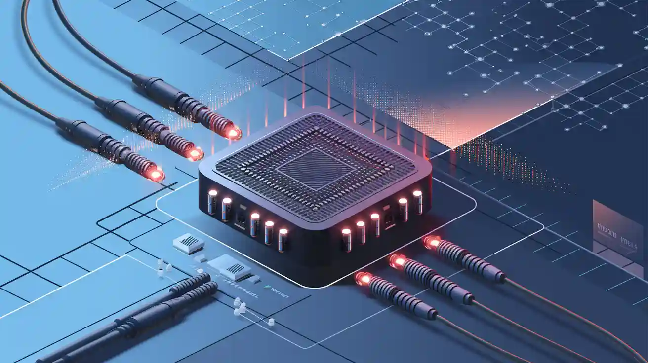
✅ LINK-PP PCB-Based Solutions
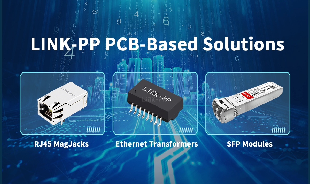
As a global supplier of magnetic components and connectors, LINK-PP integrates PCB design into high-performance networking solutions. Our products are engineered to meet the strict requirements of Ethernet connectivity, telecom equipment, and data communication systems:
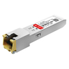
RJ45 Integrated Connectors – Built with optimized PCB layouts for Gigabit and 10G Ethernet.
Ethernet Transformers (LAN Magnetics) – Provide isolation voltage and signal integrity in high-speed circuits.
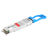
SFP/SFP28 Modules – PCB-based transceiver modules for fiber and copper applications.
By using advanced PCB design and strict quality control, LINK-PP ensures reliable connectivity across enterprise networking, automotive Ethernet, and telecom systems.
✅ Conclusion
The PCB (Printed Circuit Board) is more than just a wiring board—it is the foundation of modern electronics, enabling compact, reliable, and high-speed systems. As technology advances, PCBs are evolving to support 5G networks, IoT devices, and electric vehicles. With expertise in PCB-integrated connectors and magnetics, LINK-PP provides the building blocks for next-generation communication and computing systems.