🚀 What Is Silicon Photonics?
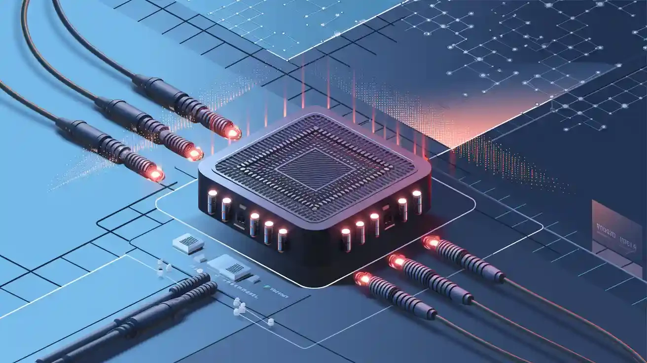
Silicon photonics (SiPh) is an advanced technology that merges silicon-based semiconductor manufacturing with photonic components for data transmission, processing, and sensing. It enables optical communication on a silicon platform, bringing together the speed of light with the scalability of CMOS electronics.
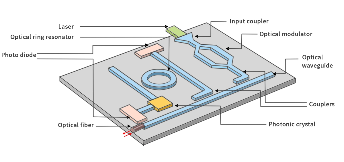
At its core, silicon photonics fabricates photonic integrated circuits (PICs) on silicon-on-insulator (SOI) substrates using similar processes to those of traditional CMOS chips. Because silicon is transparent at telecom wavelengths (around 1.3 µm and 1.55 µm) and benefits from a mature manufacturing ecosystem, it is an ideal platform for integrating waveguides, modulators, detectors, and other optical functions directly onto a chip.
🚀 Core Components of Silicon Photonics
● Waveguides and Optical Paths
Silicon waveguides confine and guide light through total internal reflection within an SOI structure. The high refractive index contrast between silicon and silicon dioxide enables strong light confinement, allowing for miniaturized and low-loss optical routing at telecom wavelengths.
● Modulators and Optical Switches
Optical modulators convert electrical signals into optical signals by varying light properties such as phase or amplitude. Common silicon photonic modulators include Mach–Zehnder interferometers and micro-ring resonators, offering high-speed performance suitable for 100 Gb/s and beyond data transmission.
● Light Sources and Photodetectors
Because silicon is an indirect-bandgap material, it cannot efficiently emit light. To overcome this, silicon photonic platforms often integrate III–V materials such as InP or GaAs for lasers, and germanium photodetectors for optical-to-electrical conversion.
● Couplers, Interfaces, and Packaging
Optical coupling between fiber and silicon is achieved via grating couplers or edge couplers, enabling seamless integration into optical networks. Advanced packaging ensures precise alignment, efficient heat dissipation, and electrical co-integration with driver ICs and transimpedance amplifiers.
🚀 Key Advantages of Silicon Photonics
▶ High Bandwidth and Low Latency
Optical carriers operate at frequencies far higher than electrical signals, supporting data rates exceeding 400 Gb/s per link with ultra-low latency—essential for AI workloads, data centers, and 5G/6G communications.
▶ Energy Efficiency and Integration
Optical interconnects consume less power than electrical counterparts, minimizing resistive losses and heat generation. Because silicon photonics is CMOS-compatible, it allows seamless co-integration of photonics and electronics on the same substrate.
▶ Scalability and Cost-Effectiveness
Leveraging the mature silicon foundry infrastructure, silicon photonics enables high-volume production and cost reduction through standardized CMOS fabrication processes.
▶ Miniaturization and Density
Tightly confined waveguides allow for compact, high-density optical circuits, supporting multi-channel, multi-wavelength systems in minimal footprint designs.
🚀 Application Domains of Silicon Photonics
1. Data Center Interconnects and High-Performance Computing
In data centers, silicon photonics is transforming rack-to-rack and chip-to-chip communication. It provides the backbone for 400G and 800G optical transceivers, offering ultra-fast, low-latency interconnects between servers and switches.
2. Telecommunications and Optical Networking
Silicon photonic transceivers are widely used in metro and long-haul networks, enabling efficient, high-capacity fiber links essential for modern communication infrastructure.
3. Sensing, Biomedical, and LiDAR Applications
Compact silicon photonic sensors are increasingly adopted in biomedical diagnostics, environmental monitoring, and LiDAR systems for autonomous vehicles due to their precision and integration potential.
4. Artificial Intelligence and Co-Packaged Optics
AI accelerators demand massive data throughput between processors and memory. Co-packaged optics (CPO) using silicon photonics places optical transceivers near compute units, minimizing latency and improving bandwidth density for AI clusters.
🚀 Challenges and Limitations
◆ Light Source Integration
Silicon cannot directly generate light efficiently, requiring heterogeneous integration with III–V materials. This adds complexity, cost, and challenges in yield optimization.
◆ Packaging and Coupling
Efficient alignment between optical fibers and silicon chips demands sub-micron precision. Packaging remains one of the most cost-sensitive and technically demanding aspects of silicon photonics.
◆ Manufacturing Yield and Scale
While silicon photonics uses mature CMOS processes, photonic devices introduce new fabrication tolerances that can affect yield and performance consistency.
◆ Thermal Management
Photonic components are temperature-sensitive, and thermal fluctuations can shift optical resonance or degrade signal integrity, requiring advanced cooling and control mechanisms.
◆ Ecosystem and Standardization
Design automation, testing, and packaging standards for silicon photonics are still evolving. Collaboration between foundries, design houses, and module vendors is essential for ecosystem maturity.
🚀 Relevance for LINK-PP SFP Modules
As a professional manufacturer of high-speed connectivity solutions, LINK-PP can leverage silicon photonics trends to enhance product innovation in optical interconnects and transceiver modules.
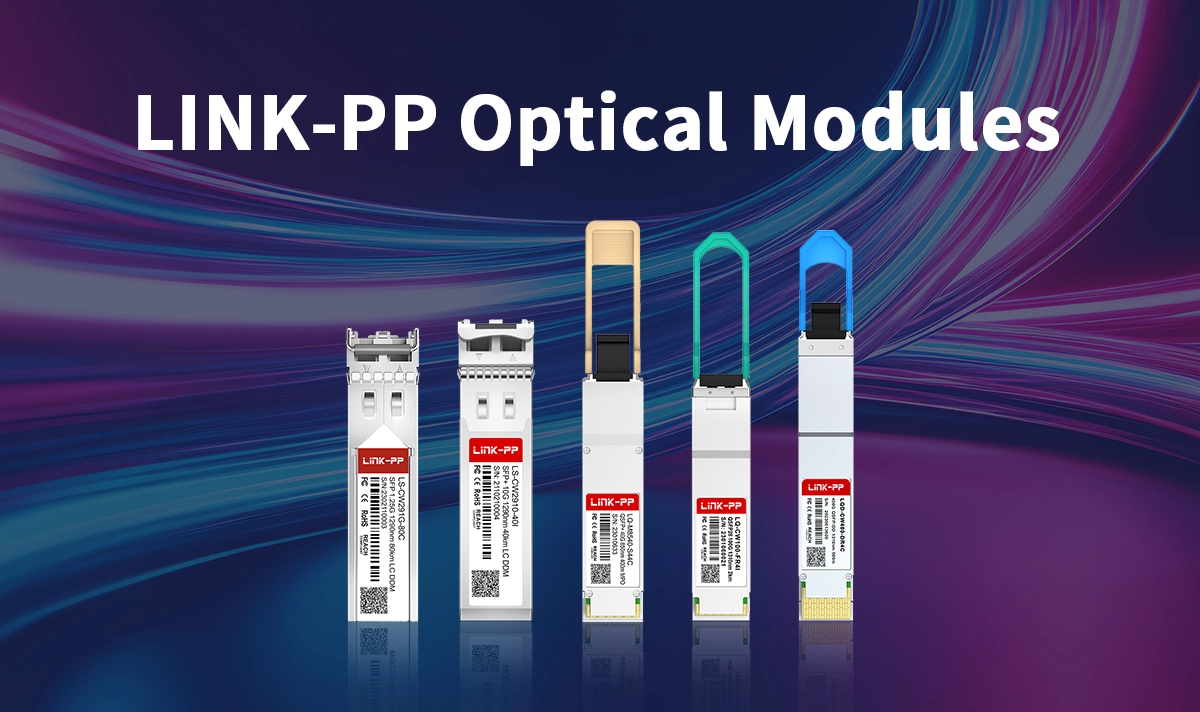
Optical Transceivers: Silicon photonics-based 400G/800G transceivers provide the optical foundation for next-generation data center interconnects. LINK-PP’s product portfolio, such as SFP optical transceivers, complements these high-speed optical platforms.
Hybrid RJ45 and Optical Solutions: Combining optical and copper interconnects supports hybrid network topologies in AI computing and edge devices.
eCPRI/CPRI Compatibility: LINK-PP’s components can be integrated into front-haul and mid-haul networks using silicon photonic modules for 5G/6G infrastructure.
By aligning products with silicon photonics applications, LINK-PP strengthens its position in high-performance, low-latency network interconnect markets.
🚀 Frequently Asked Questions
Q1. What wavelengths does silicon photonics operate at?
Typically at 1.3 µm and 1.55 µm, corresponding to low-loss windows of standard optical fiber communication.
Q2. Is every optical transceiver based on silicon photonics?
No. Many transceivers still use discrete III–V components, but silicon photonics is rapidly growing due to cost and integration benefits.
Q3. Can silicon photonics replace electrical interconnects entirely?
Not fully yet. Short-reach links still rely on copper for cost and simplicity, but optical links dominate high-speed, long-reach data transmission.
🚀 Conclusion
Silicon photonics is redefining how data moves across chips, servers, and networks. By merging the scalability of silicon with the speed of light, it offers a clear path toward higher bandwidth, lower latency, and better energy efficiency.
While integration and packaging challenges persist, the technology’s momentum across AI computing, cloud infrastructure, and optical networking ensures it will be a cornerstone of next-generation communication systems. For LINK-PP, embracing silicon photonics in both product development and content strategy represents a forward-looking step toward the future of high-speed connectivity.