🔹 Understanding CMOS Technology
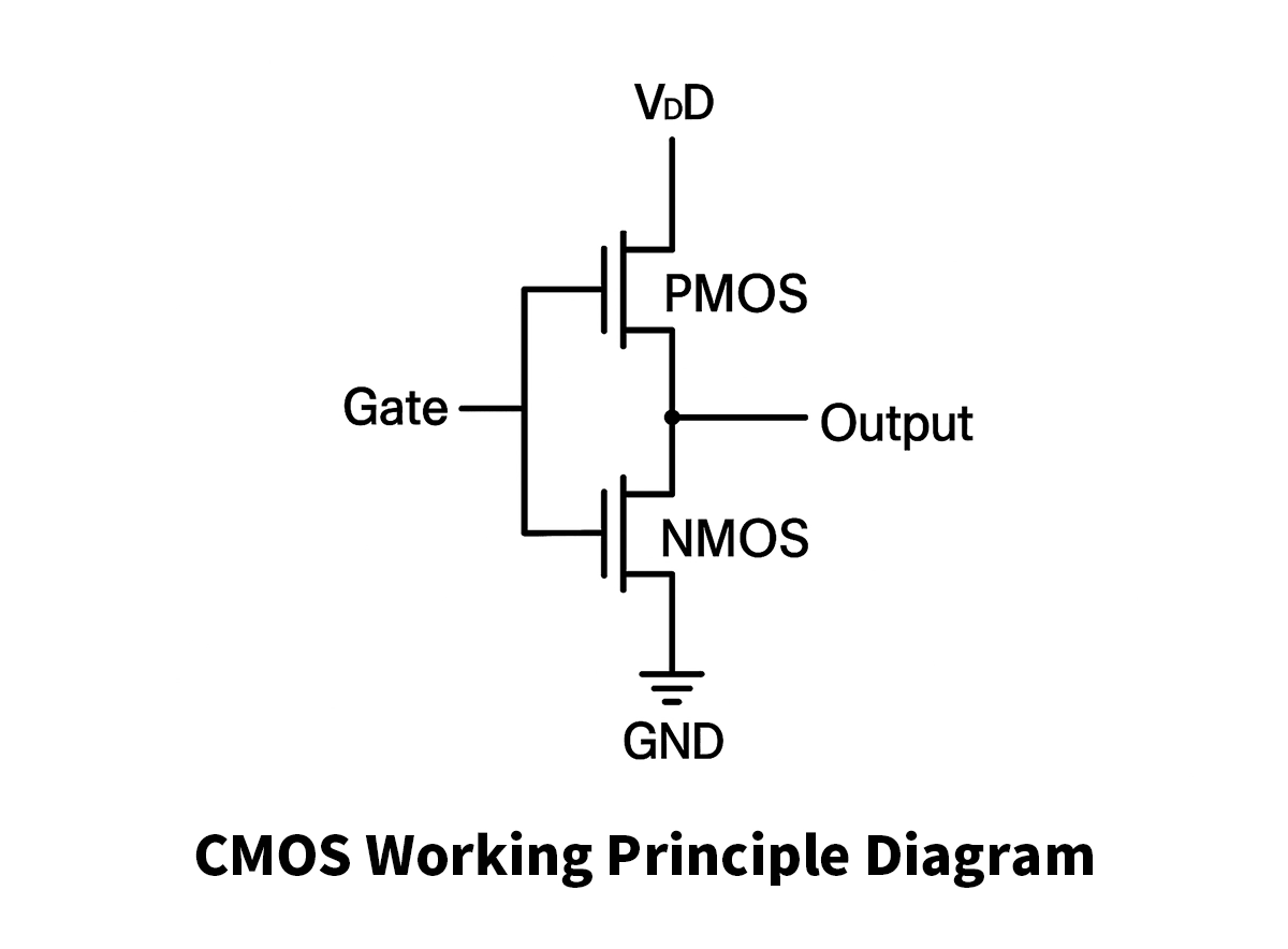
CMOS (Complementary Metal-Oxide-Semiconductor) is the dominant semiconductor fabrication technology used in integrated circuits. It employs complementary pairs of p-type (PMOS) and n-type (NMOS) transistors to construct digital logic, analog, and mixed-signal circuits. The “complementary” configuration ensures that when one transistor conducts, the other is off, resulting in extremely low static power consumption — a key factor behind CMOS’s efficiency and popularity in modern electronics.
CMOS technology underpins nearly every type of chip found in today’s devices, including microprocessors, memory chips, sensors, and communication ICs.
🔹 How CMOS Works
Complementary Transistor Operation
In CMOS logic, PMOS transistors pull the output high while NMOS transistors pull it low. This complementary design eliminates steady-state current flow except during switching, drastically reducing power usage compared to older NMOS or TTL logic designs.
Device Structure
The term Metal-Oxide-Semiconductor refers to the MOSFET structure:
Metal gate (modern devices often use polysilicon or metal gates)
Oxide layer (a thin dielectric that insulates the gate)
Semiconductor substrate (typically silicon)
Advances in CMOS manufacturing — from planar transistors to FinFET and gate-all-around (GAA) structures — have enabled continual scaling in speed, power efficiency, and transistor density.
🔹 Key Advantages of CMOS
Feature | Description |
|---|---|
Low Power Consumption | Minimal static current when idle, only dynamic power during switching. |
High Integration Density | Enables billions of transistors per chip for compact and powerful ICs. |
Noise Immunity | Stable signal transmission and high reliability under various conditions. |
Mature Manufacturing Process | Extensive foundry and design tool support, ensuring consistent quality. |
Design Trade-offs
While CMOS provides outstanding energy efficiency, dynamic power rises with clock frequency and load capacitance. At advanced nodes, leakage and process variability also require careful design strategies to maintain performance and yield.
🔹 CMOS Image Sensors vs. CCD
Architecture and Working Principle
A CMOS image sensor integrates amplifiers and often ADCs (analog-to-digital converters) directly on each pixel or column, enabling fast readout and low power operation. In contrast, a CCD (Charge-Coupled Device) transfers charge sequentially across the chip to a single readout node, offering lower noise but slower speeds.
Feature | CMOS Sensor | CCD Sensor |
|---|---|---|
Power Efficiency | Low | High |
Speed | Fast (random access) | Slow (sequential readout) |
Integration | On-chip signal processing | External readout circuits |
Applications | Smartphones, automotive, surveillance | Scientific imaging, astronomy |
CMOS sensors dominate in applications where power, cost, and integration matter most, while CCDs persist in niche high-end imaging where low noise remains critical.
🔹 CMOS in Silicon Photonics
Integration of Electronics and Photonics
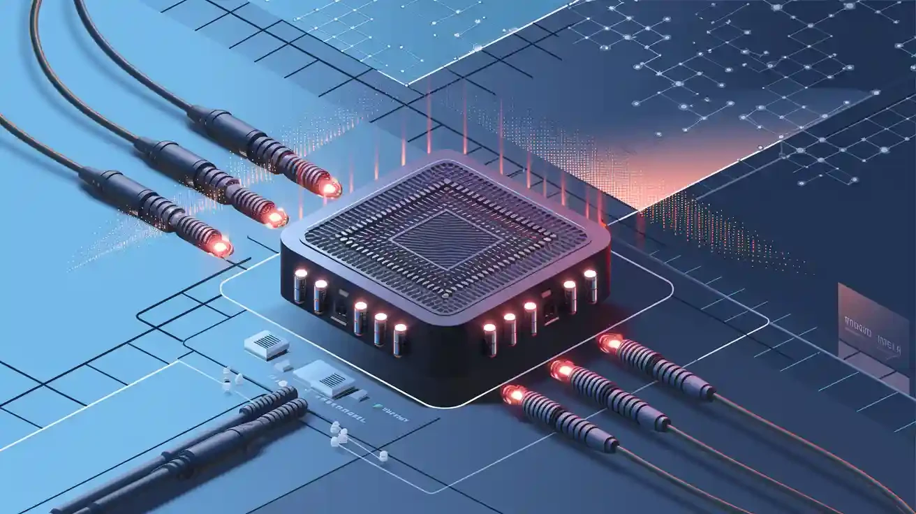
The convergence of CMOS and silicon photonics enables high-speed optical communication within data centers, telecom systems, and AI infrastructure. Silicon photonics integrates optical waveguides, modulators, and detectors onto a silicon substrate, while CMOS circuitry provides essential electronic functions — such as drivers, amplifiers, and control logic.
Key Integration Benefits
Power Efficiency: CMOS-based drivers and TIAs (transimpedance amplifiers) minimize power per bit transmitted.
Compact Form Factor: Co-packaged photonics and CMOS reduce board space and latency.
Scalability: CMOS-compatible processes lower manufacturing costs and support volume production.
This synergy between CMOS and photonics forms the foundation for next-generation optical transceivers and high-speed communication modules.
🔹 CMOS in Optical Transceivers
CMOS electronics play a central role in optical transceiver design, providing signal processing, power regulation, and data conversion functions within optical modules.
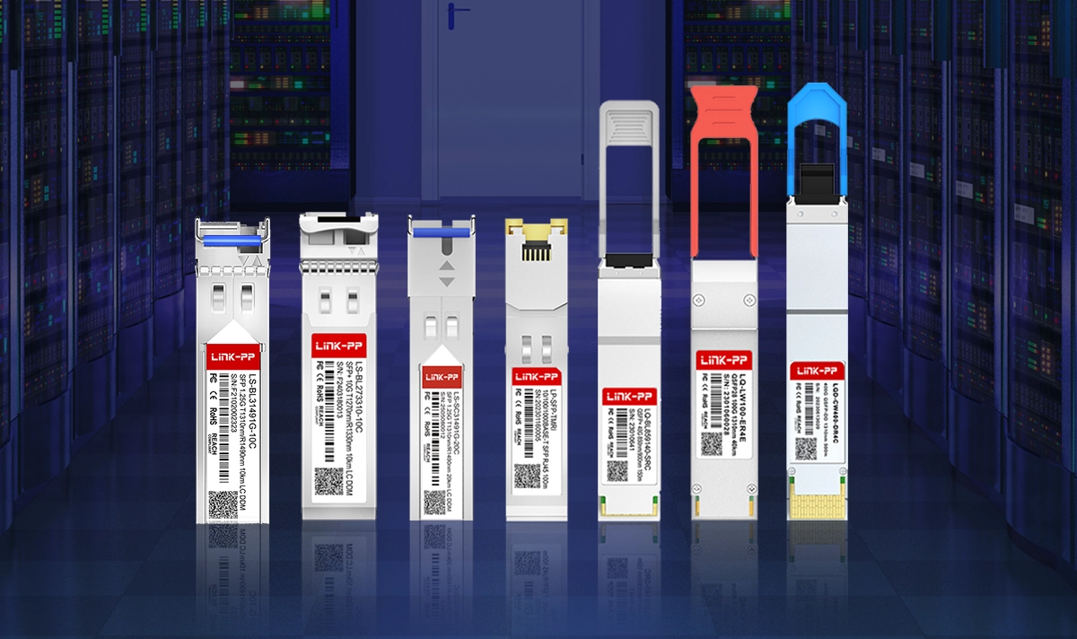
LINK-PP offers a full range of optical transceivers — including SFP, SFP+, and QSFP modules — that leverage CMOS-based control ICs to support reliable, low-power data transmission across Ethernet and telecom networks.
For example, LINK-PP optical modules combine CMOS driver chips, laser diodes, and photodetectors into a single compact solution, supporting data rates up to 400G with excellent signal integrity.
🔹 Applications of CMOS Technology
Memory: SRAM, Flash, and embedded DRAM
Imaging: Consumer and industrial CMOS sensors
RF Circuits: Wireless communication and transceiver ICs
Optical Communication: CMOS-based SerDes, TIA, and driver ICs in silicon photonic systems
🔹 FAQs
Q1. Is CMOS the same as a MOSFET?
No. A MOSFET is a type of transistor. CMOS refers to a circuit design and manufacturing process that uses complementary pairs of MOSFETs (PMOS + NMOS).
Q2. Why is CMOS considered low-power?
Because only one of the two transistors conducts at any given time, static power consumption is nearly zero. Power is primarily consumed during signal transitions.
Q3. How is CMOS used in optical transceivers?
CMOS circuitry drives modulators, amplifies received signals, and manages control logic within optical transceivers, ensuring efficient, high-speed data transfer.
🔹 Conclusion
CMOS remains the core technology of modern electronics, combining high speed, low power, and scalability across applications from microprocessors to silicon photonics. Its integration with optical technologies enables a new generation of high-bandwidth, energy-efficient systems for data centers, 5G/6G networks, and intelligent infrastructure.
For advanced optical connectivity built on CMOS precision and reliability, explore the LINK-PP Optical Transceiver Series — designed to support the evolving demands of high-speed communication systems.