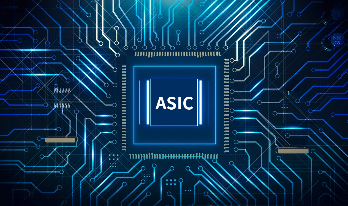
🔍 Overview: an application-specific integrated circuit, or ASIC, is a microchip made for a special job. Unlike general-purpose chips, an application-specific integrated circuit does only one thing and does it very well. ASICs are now very important in devices that need to be fast or use little power. Many industries pick an asic because it can work better and save energy. Let’s dive into the world of ASIC! Discover what ASICs are, how they revolutionize everything from your smartphone to supercomputers and Bitcoin mining, why they outperform generic chips, and where cutting-edge solutions like LINK-PP optical transceivers leverage their power. Master the tech behind the speed!
➤ What Exactly is an ASIC (Application-Specific Integrated Circuit)?
An ASIC is a custom-built integrated circuit (IC) designed and manufactured for a very specific application or function. Unlike general-purpose processors (CPUs, GPUs) or programmable logic devices (FPGAs), which can be configured for various tasks via software or firmware, an ASIC chip is hardwired during its fabrication process to perform its dedicated function with unparalleled efficiency. Think of it as a tailor-made suit versus off-the-rack clothing.
How ASICs Work: Dedication at the Silicon Level
The magic of an ASIC lies in its optimized physical design:
Specificity: The entire circuit layout – every transistor, connection, and logic gate – is meticulously crafted solely to execute its target task.
Hardwired Logic: The functionality is fixed in the silicon. There’s no overhead for fetching and interpreting general instructions.
Optimization: Designers can aggressively optimize for key metrics like performance (speed), power consumption, physical size (die area), and cost for high-volume production, precisely because the scope is narrow.
➤ ASIC vs. FPGA: Choosing the Right Tool (Key Differences Table)
While both serve specialized computing needs, ASICs and FPGAs (Field-Programmable Gate Arrays) are fundamentally different. Understanding this is crucial for ASIC design services or selecting hardware components like high-speed optical transceivers.
Feature | ASIC (Application-Specific IC) | FPGA (Field-Programmable Gate Array) |
|---|---|---|
Customization | Fully Custom (Tailor-made silicon) | Configurable (Prefab logic blocks + interconnect) |
Design Stage | Fabrication (Irreversible) | Post-Manufacture (Loadable configuration bitstream) |
Performance | ✅✅✅ Highest (Optimized, no overhead) | ✅✅ High (But has config overhead) |
Power Consumption | ✅✅✅ Lowest (Minimal wasted power) | ✅✅ Moderate to High (Configuration power) |
Unit Cost (High Vol) | ✅✅✅ Lowest (After NRE amortized) | ✅ Moderate to High |
Unit Cost (Low Vol) | ❌ Very High (Due to NRE) | ✅✅ Lower (No significant NRE) |
Non-Recurring Engineering (NRE) | ❌ Very High (Design, masks, tooling) | ✅✅ Low/None (Standard parts) |
Time-to-Market | ❌ Long (Design, fab, testing) | ✅✅✅ Short (Design & configure) |
Flexibility | ❌ None (Function fixed at fabrication) | ✅✅✅ High (Re-programmable) |
Best Suited For | Ultra-high volume, performance-critical, power-sensitive fixed functions | Prototyping, lower volume, evolving standards, need for field updates |
➤ Why ASICs Dominate: Unleashing Unmatched Advantages
The ASIC advantage manifests in several critical areas, driving their adoption across industries:
⚡️ Blazing Speed & Performance: By eliminating the overhead of instruction fetching, decoding, and executing generic operations, ASICs execute their specific function directly in hardware. This results in raw processing speeds often orders of magnitude faster than software running on a CPU or even an FPGA for the same task. Think cryptocurrency mining ASICs or network processing ASICs handling terabits of data.
🔋 Ultra-Low Power Consumption: Optimized silicon means only the essential transistors switch, minimizing wasted energy. This is paramount for battery-powered devices (IoT sensors, wearables) and massive data centers where power efficiency translates directly to operational cost and sustainability.
📏 Miniaturization: Integrating complex, highly optimized functionality onto a single, compact chip saves significant board space. This is critical for consumer electronics (smartphones, tablets) and densely packed hardware like network switches and optical transceiver modules.
💰 Cost Efficiency (At Volume): While initial design (ASIC design cost) and manufacturing setup (NRE costs) are high, the per-unit cost of a mass-produced ASIC plummets significantly below that of an equivalent FPGA solution. High-volume applications reap substantial savings.
🛡️ Enhanced Security: The fixed, opaque nature of the silicon makes reverse-engineering the functionality significantly harder than analyzing software or FPGA configurations, offering a layer of hardware security for sensitive applications.
➤ Where ASICs Power Our World: Key Applications
ASICs are ubiquitous, silently driving innovation:
📱 Consumer Electronics: Image signal processors (ISPs) in phone cameras, audio codecs, touch controllers, display drivers, sensor hubs.
🌍 Networking & Telecommunications: High-speed network ASICs in routers/switches (handling packet forwarding, traffic management, security – deep packet inspection ASIC), SerDes (Serializer/Deserializer) cores, baseband processors (4G/5G), and crucially, within optical modules.
💰 Cryptocurrency & Blockchain: ASIC miners (like Bitcoin ASICs) are purpose-built for the intense, specific computations required for proof-of-work mining, vastly outperforming CPUs/GPUs.
🤖 Artificial Intelligence & Machine Learning: AI accelerators and Tensor Processing Units (TPUs) are specialized ASICs designed to perform massive matrix multiplications and neural network inference with extreme efficiency.
🚗 Automotive: Engine control units (ECUs), advanced driver-assistance systems (ADAS), radar/lidar processing, infotainment controllers.
⚙️ Industrial Automation: Motor controllers, robotics control, programmable logic controller (PLC) functions.
🩺 Medical Devices: Imaging equipment (MRI, CT scan processing), implantable devices, diagnostic tools.
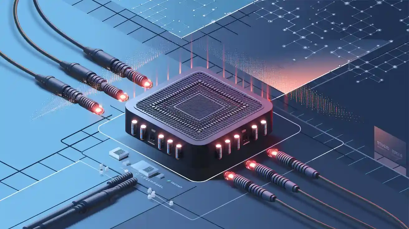
➤ ASICs in Networking & Optical Modules: The Speed Enablers
This is where the ASIC meaning translates directly to the backbone of the internet and data centers. Modern high-speed networking (100G, 200G, 400G, 800G+) relies heavily on specialized network processor ASICs and ASIC-based optical modules.
The Challenge: Moving terabits of data requires incredibly fast, low-latency processing within strict power and thermal budgets. Generic processors simply can’t keep up.
The ASIC Solution: Networking ASICs handle critical tasks like:
Packet classification, forwarding, and routing at line rate.
Traffic shaping and Quality of Service (QoS) enforcement.
Deep Packet Inspection (DPI) for security and analytics.
Advanced encryption/decryption (e.g., MACsec, IPsec).
Precise timing synchronization (e.g., PTP).
Optical Modules & ASICs: Inside every advanced optical module (SFP+, QSFP28, QSFP-DD, OSFP), an ASIC is the brain. These optical transceiver ASICs perform essential functions:
Gearboxing: Converting data rates between the host interface (e.g., 50G PAM4 electrical lanes) and the optical engine’s native rate.
CDR (Clock and Data Recovery): Extracting a clean clock signal and retiming the data from the noisy incoming electrical signal.
Laser Driver Control: Precisely modulating the laser diode current.
APD/TIA Control (Receiver): Managing the avalanche photodiode (APD) bias and transimpedance amplifier (TIA) for optimal sensitivity.
Digital Diagnostics Monitoring (DDM/DOM): Continuously monitoring and reporting parameters like temperature, voltage, laser bias current, transmitted/received optical power via the host interface.
Encoding/Decoding: Implementing standards like FEC (Forward Error Correction – e.g., Reed-Solomon FEC, KP4 FEC, Firecode FEC) to detect and correct transmission errors, crucial for maintaining signal integrity over long distances or challenging links. Low-latency FEC ASIC blocks are vital for high-performance computing (HPC) and financial trading applications.
Signal Conditioning: Equalization (CTLE, DFE) to compensate for signal degradation over the electrical traces and cables.
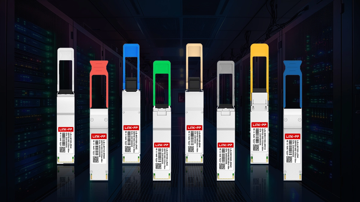
💡 The LINK-PP Advantage: Leading manufacturers like LINK-PP integrate highly sophisticated, custom ASICs into their optical modules. For instance, the LINK-PP 400G QSFP-DD DR4 module leverages a purpose-built ASIC optimized for low power, high signal integrity, and robust FEC ASIC implementation, ensuring reliable 400Gbps transmission over demanding distances. This focus on custom ASIC design within optical transceivers directly translates to superior performance, reliability, and power efficiency for critical data center and telecom infrastructure. When discussing optical module compatibility or high-speed interconnect solutions, understanding the role of the internal ASIC is key.
➤ The Future of ASICs: More Specialization, Chiplets, and AI
The ASIC revolution continues:
Hyper-Specialization: ASICs will become even more tailored for niche applications (e.g., domain-specific AI accelerators, ultra-low-power IoT edge processors).
Chiplet-Based ASICs: Leveraging Multi-Die Integration and Chiplet technology to combine smaller, specialized “chiplets” (potentially from different process nodes) into a single package. This offers flexibility, potentially lowers costs for certain designs, and improves yield compared to monolithic designs. Universal Chiplet Interconnect Express (UCIe) is a key enabling standard. Heterogeneous integration is key.
AI-Driven Design: Machine learning will increasingly optimize ASIC design flows, accelerating P&R, power analysis, and verification, reducing time-to-market and improving PPA.
Advanced Packaging: Technologies like 2.5D/3D integration (using silicon interposers or through-silicon vias – TSVs) will be crucial for integrating diverse chiplets and memory (HBM – High Bandwidth Memory) tightly together, overcoming traditional interconnect bottlenecks. This is vital for next-gen AI ASICs and high-performance computing ASICs.
Co-Packaged Optics (CPO): Moving the optical engine (and potentially its driving ASIC) closer to or even onto the same package as the switch ASIC, dramatically reducing power consumption and increasing bandwidth density for next-gen data centers. ASICs are central to enabling CPO.
➤ Conclusion: The Indispensable Engine of Optimization
ASICs (Application-Specific Integrated Circuits) are not just another chip; they are the pinnacle of hardware optimization for specific, demanding tasks. By sacrificing flexibility, they achieve unmatched performance, power efficiency, miniaturization, and cost-effectiveness at scale. From powering the AI revolution and securing blockchain networks to enabling the blazing-fast optical modules (like LINK-PP’s 400G modules) that form the internet’s backbone, ASICs are fundamental to technological progress. Understanding what an ASIC is, its advantages and disadvantages compared to alternatives like FPGAs, and its intricate design and manufacturing process is crucial for engineers, designers, and technology decision-makers navigating the landscape of high-performance computing and connectivity.
Ready to harness the power of ASIC-optimized performance in your network?
👉 Explore LINK-PP’s cutting-edge portfolio of ASIC-driven optical modules designed for maximum reliability, efficiency, and speed. Discover how our custom ASIC solutions in products like the LINK-PP 400G QSFP-DD DR4 and LINK-PP 800G OSFP modules can future-proof your infrastructure.
For expert advice, Contact our Technical Team today ➞